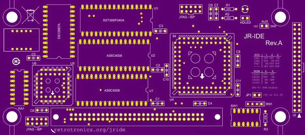
Front side PCB rendering of the circuit board. The first two runs were ordered from OSHPark – hence the purple solder mask and ENIG finish.
Overview
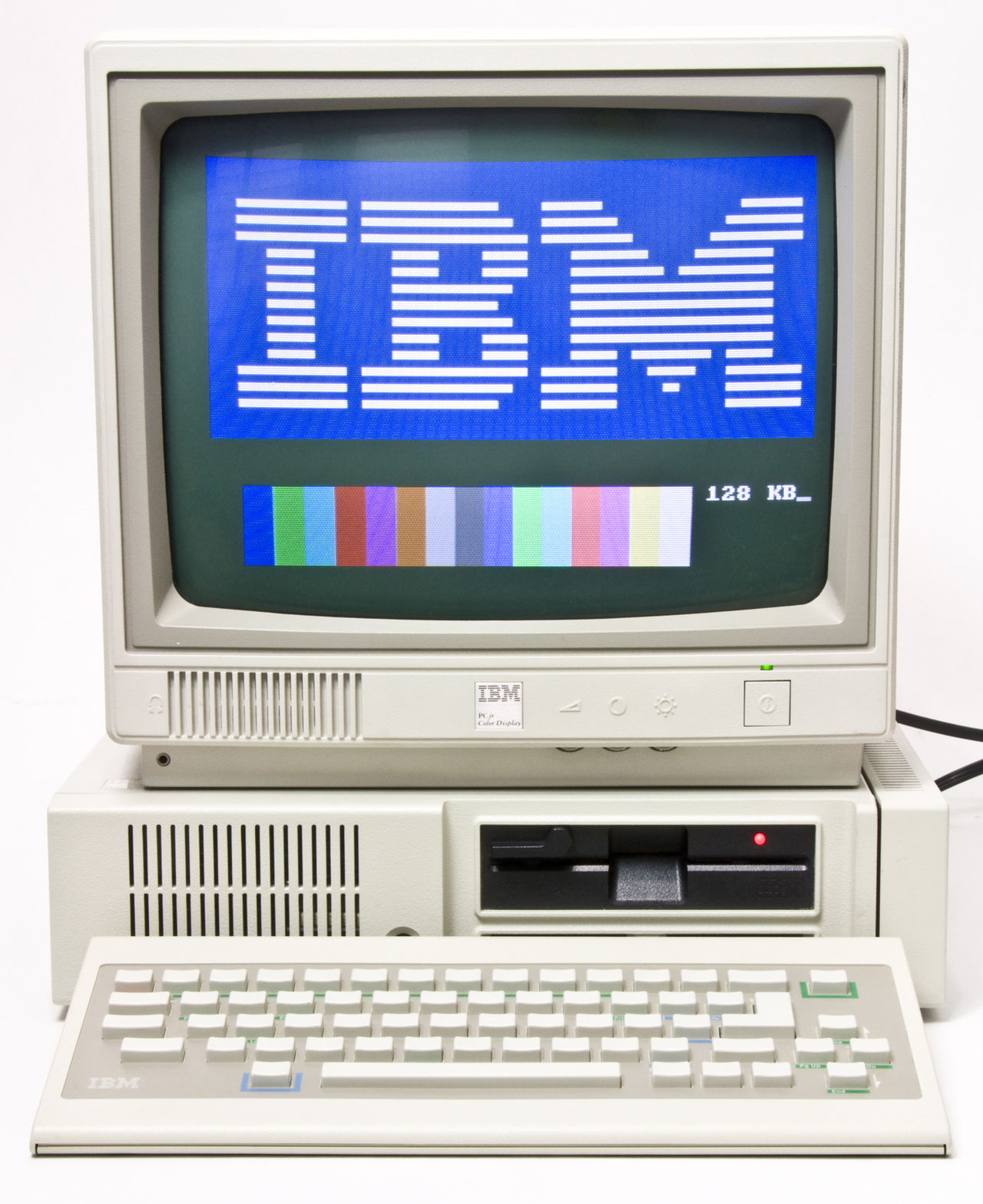
jr-IDE is an open-source kit designed for the IBM model 4860 “PC Jr” that includes the following features on a sidecar board:
- 40-pin Parallel ATA IDE interface
- 1MB of static RAM
- 512KB of flash ROM
- A real-time clock
- A Power On Self Test (POST) display
- Bus activity indicator LED
The board includes pass-through mounting holes allowing it to fit into a standard IBM sidecar enclosure. The IBM PC Jr sidecar bus connectors (AMP 532773-2 & 532771-2) are very hard to find parts. If you purchase the complete parts kit, a matted pair is included. The only thing you must supply yourself is a donor shell from another side-car. Many people use the parallel port side-car commonly found on eBay. The process is completely reversible if you decide to remove the jr-IDE from your system and return the shell to it’s donor card as long as you follow the assembly notes below.
The project genesis happened on Mike’s terrific PC Jr forums in this thread:
http://www.brutman.com/forums/viewtopic.php?f=1&t=180
Many forums members came up with the idea and were already refining the concept when I joined. I used the project as an experiment project to better my understanding and use of Atmel’s ATF150x CPLD parts. More on those below.
Hardware
The primary design goals were simple:
- Provide a functional and bootable 40-pin IDE hard-disk interface
- Protect for hobby friendly assembly – meaning restrict part choices to platted through-hole mounting. No surface mount soldering.
Extra RAM, ROM, and many more features were considered secondary.
IDE Interface
The original inspiration for the board was to bring the extremely popular XT-IDE project to a PC Jr compatible form factor. The XT-IDE project was also the foundation for the above design goals. Parallel ATA (or PATA) is a 16-bit interface standard developed long after legacy 8-bit machines like the IBM 5150 PC and the 4680 Jr were obsolete. 8-bit partial register accesses are not allowed in the PATA specification. So how do you allow an 8-bit machine to access 16-bit registers atomically?
The original XT-IDE project was inspired by Tilmann Reh’s excellent work on the Generic Z80 IDE Interface (GIDE). He and the original designers of the XT-IDE project had already worked out the answer. You perform consecutive 8-bit accesses to read both bytes. The initial 8-bit read triggers a 16-bit IDE read holding the upper byte in a latch and returning the lower byte on the bus. The second 8-bit read brings in the upper byte from the latch. Writes work in a similar fashion. The initial 8-bit write places the lower byte in a latch. The second 8-bit write triggers a 16-bit IDE write presenting the upper byte from the bus and the lower byte from the latch. Since the CPU in the PC and it’s compatibles like the PC Jr is an Intel 8088 – a 16-bit CPU, multi-byte reads and writes are automatically generated when performing a 16-bit memory or I/O operation at a register level. However the address presented for the successive byte is incremented by one. So some adjustment must be done in register address offsets making any software written for legacy 16-bit IDE adapters incompatible with these new types of 8-bit cards.
The original PATA/IDE cards placed the register file in the I/O port space with each 16-bit register at consecutive I/O addresses. The XT-IDE project also decoded the register file in the I/O port space. However due to the byte-wise addressing and transfer scheme employed to read the 16-bit IDE registers atomically, the address mapping was altered. Since the 8088 is a little endian machine, lower bytes were placed at even addresses. Upper bytes were placed at odd addresses. The I/O port address is shifted down by 1 bit before passing as the IDE register address to the drive. Thus any of the XT-IDE or derivative cards are only compatible with standard PATA/IDE cards at a BIOS level and not a hardware level.
CPLDs
The original XT-IDE was implemented with discrete industry standard 74xx series TTL devices. Primarily so that project builders can assemble the board with just a soldering iron – ie. are not required to have any special programming hardware. I however had a different motive in my part choices. I chose to use CPLDs to lower component count and – in theory- reduce cost. CPLDs are Complex Programmable Logic Devices. But trust me, they are not that complex. I see many board designs using discrete logic. Each chip used carries a packaging premium and usually a socket cost since most owners would like an easily repairable board. The main drawback to the CPLD approach is unfortunately the same – cost; but for different reasons. The ATF150x series CPLDs are aftermarket functional reproductions of Altera’s MAX7000 line. The 5 volt and through-hole friendly packages (PLCC) versions of the ATF150x family are not in high demand and thus carry a price premium (along with price volatility and availability). However the raw number of chips a CPLD can reduce from a design is significant – and so is the board area. The Atmel series devices can also be programmed via a PC parallel port using a ByteBlaster II compatible cable that can be found on eBay for a low as $15 shipped to the US. So the programming requirement is still relatively hobby friendly. Most builders just buy them pre-programmed in kits from me.
Since an 8-bit latching IDE interface can never be strictly hardware compatible with a genuine IDE card, I was free to take certain hardware liberties to improve performance that would be masked with set of Int13h BIOS compatible software calls. Most notable of these changes is to map the IDE register file into the memory address space instead of the I/O. This allows for fewer wait states compared to 8-bit ISA I/O port reads/writes. I also virtualizing logical block transfers to/from the card. Both of these performance changes would add additional decode logic to a discrete chip design. However they just consumed extra gate capacity in a CPLD design.
Two CPLD are used in the jr-IDE design mainly because I ran out of I/O pins on the first 84-pin device. It still has spare logic capacity. The primary ATF1508 handles the IDE interface, RAM decode, ROM decode and paging, and preliminary I/O decode for the second CPLD. The secondary ATF1504 handles the POST display (dual hex to 7-segment decoders and PWM drive) and decode and strobe setup for the Real-Time Clock (RTC) chip.
Memory Mapped I/O
Normal IDE transfers are setup through control registers by passing the CHS address you want to read or write to the IDE drive, waiting for a busy flag to clear meaning the read is done or its ready to receive write data, and then peeking or poking 512 bytes worth of a block in to or out of an I/O port data register. This is known as PIO or Port I/O mode. Other more advanced features of the IDE interface allow streaming of blocks over a DMA based timing scheme. However the minimum PIO performance timings in the 1.0 ATA specification are above the max bandwidth numbers for ISA. So the slow bottleneck in any design will be the ISA bus itself. On an 8088 things are even worse. The 8088 has no instruction cache. It only has a 4 byte instruction pre-fetch pipe. So the number of instructions needed to fetch each byte from the I/O port and then store them to memory is also significant – especially when you consider the number of bus cycles they consume verses the actual transfer of block data from the drive.
Later Intel processors added string instructions for the I/O port space. A ‘rep insw’ instruction would be fetched once by the processor and continually perform bus data transfers until a counter register hit zero. However it does not exist on 8088/8086 processors. Cards could also use a DMA request line to cause the 8237A DMA controller to perform sequential I/O to memory bus cycles without needing to fetch instructions telling it how to do the work. However DMA adds even more logic and logic signal to a design. The 8088 does however have string instructions for memory primarily used for memory to memory copies without causing a lot of intermediate instruction fetches. Thus if the IDE data register is decoded at 512 consecutive memory locations, a ‘rep movws’ could be used to quickly transfer a block of data between main memory and the IDE interface efficiently and thus quickly.
This is the pseudo code with normal port based I/O:
loop:
    inp:
        - instruction fetch
        - data fetch from I/O port to a register
    stosb:
        - instruction fetch
        - data write from register to memory
    dec counter:
        - instruction fetch
    jnz loop:
        - instruction fetch
New pseudo-code with memory mapping:
rep movsw:
        - instruction fetch only on first iteration
        - data fetch from port
        - data write to memory
By using ‘rep movsw’ and making the IDE data register span 512 consecutive byte addresses, performance was improved from 60-80 KB/s on an IBM 5150 to 330-350 KB/s on the PC Jr!
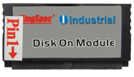
Kingspec Industrial Disk-on-Module (DoM) used by many jr-IDE owners
Compatibility and Drive Power
The board features a standard 40-pin IDE header. From the IDE header you can run a cable to a standard 3.5 inch IDE hard drive, use a wiring adapter to connect a 2.5 inch IDE hard drive, or use a FLASH based product such as a CF card with an adapter or a Disk On Module (DOM). Power for small devices (CF cards or DOM) is available on the card via a jumper that routes +5 volts to pin 20 on the IDE connector (normally a missing key pin). Many Disk-on-Modules support powering the device from pin 20 without the use of a dedicated power cable. Power for larger devices (real IDE drives) should be provided by an external power source or a modification to the PCjr. Modern hard drives don’t require a lot of power but remember that the original internal PC Jr power supply was only rated at 70W and has only a small allowance for side-cars. The jr-IDE board does have an aux power connector with +5V and ground. However I recommend you installing a PC Jr power side-car before the jr-IDE if you solder on a cable to the aux header to provide drive power to a real physical hard drive.
For an up-to-date list of test device compatibility, please visit the jr-IDE information page at Mike’s PC Jr site: Michael Brutman’s PCjr Page
1 MB Static RAM (SRAM)
The jr-IDE board includes two Alliance 512 KB Static RAM parts. The primary CPLD performs the logic decode. This memory can be used to back-fill conventional RAM. Because the PC Jr has it’s own on-board enhanced CGA video controller, integration of video BIOS with the system BIOS, and the (relative) inability to add MDA cards, the conventional memory pool can be filled all the way to 736KB where the traditional CGA video window starts (B8000). However the default system BIOS will only count up to 640 KB without a modification. The jrCONFIG.SYS driver can be used to raise the BIOS reported memory ceiling as well as relocate the on-board video window as low as possible giving more than 700 KB of usable conventional RAM to DOS.
In addition, RAM pages can be enabled for Upper Memory Blocks (UMBs) through a dedicated control register located at offset +0x3c10 in the BIOS ROM window:
| Bit | Memory Range | Notes |
| 0 | RAM fill enable 0xC0000 -> 0xC3FFF | |
| 1 | RAM fill enable 0xC4000 -> 0xC7FFF | |
| 2 | RAM fill enable 0xC8000 -> 0xCBFFF | |
| 3 | RAM fill enable 0xCC000 -> 0xCFFFF | |
| 4 | RAM fill enable 0xD0000 -> 0xD7FFF | Must replace ZM56 decode ROM on mainboard |
| 5 | RAM fill enable 0xD8000 -> 0xDFFFF | Must replace ZM56 decode ROM on mainboard |
| 6 | RAM fill enable 0xE0000 -> 0xE7FFF | Must replace ZM56 decode ROM on mainboard |
| 7 | RAM fill enable 0xE8000 -> 0xEFFFF | Must replace ZM56 decode ROM on mainboard |
Unfortunately none of the upper memory blocks are very usable at the moment. There is a lack of formal driver support for the 48KB that would normally be available in the ‘C’ segment (64KB – jr-IDE 16KB BIOS window). The intent was the card BIOS would detect which of the 16KB ranges it was executing from in the ‘C’ segment and turn on RAM fill for the other 3. However that is not currently implemented in the option BIOS nor is the UMB DOS driver support. The ‘D’ and ‘E’ segments, which are normally reserved for PC Jr cartridge ROMs, are gated off to the side-car connector by a 8-bit ROM located on the main board marked ZM56. I have successfully de-soldered this ROM and replaced it with a 22V10 simple PLD to enable these UMBs. You can read more about those efforts in this thread:
http://www.brutman.com/forums/viewtopic.php?f=1&t=377
Note if you are making changes to the option BIOS to support the ‘C’ segment UMB back-fill, please note an optional pan’able ROM window can also be mapped into any of the 4 locations. Both must not be enabled at the same time. See the next section for more detail.
512KB Flash ROM
Flash was chosen over EEPROM for it’s inability to be affected by stray writes into the option ROM area and for better density options. The XT-IDE uses EEPROM and must write protect the ROM with a jumper. Write protection could be done via a register bit on jr-IDE, however flash parts are common in 32-pin JEDEC packages, offer stray write protection, and come in much larger sizes. Any 32-pin JEDEC compatible flash device can be used, however they commonly come in 128K, 256K, and 512K capacities. The first 14.5 KB of the flash is always reserved for the 14.5 KB of code space mapped into the Option ROM BIOS area. This 16 KB window can be any of the 4 likewise aligned addresses in the ‘C’ segment as determined by the jr-IDE DIP switch settings (C0000, C4000, C8000, or CC000).
The remainder of the flash could be used for anything. However there is no current support in the BIOS for it. Some possibilities include adding another virtual hard-disk (eg. Drive C: or D:) that maps to a FAT formatted image in the remaining 497.5 KB. This image could even be bootable allowing for DOS-in-ROM as long as the Microsoft and IBM copyrights were respected by the project and it’s users. Other options include a non-bootable ROM disk or the storage of PC Jr Cartridge ROM images. The BIOS could present a boot menu of cartridge ROMs and upon selection copy the code into a lower memory segment and execute. Or if the ZM56 modification described above was made, it could copy them into their normal ‘D’ or ‘E’ segments before execution.
To access the remaining 497.5 KB of flash, a second 16 KB memory range must be enabled in the ‘C’ segment via special register write. Once turned on, this 16 KB ROM window can be panned around to view different 16 KB pages of flash including page 0 where the Option ROM BIOS code is located. This is also how programming software can write the needed preamble writes used to erase or reprogram flash pages. The intention for any driver software making use of the extended ROM window is to:
- First disable interrupts
- Locate a 16 KB frame in the ‘C’ segment not filled by the Option ROM BIOS
- Disable RAM fill in that frame
- Enable the ROM window in that frame
- Set the page address to be accessed
- Perform the ROM accesses
- Disable the ROM window in that frame
- Re-enable RAM fill in that frame
- And finally re-enable interrupts
Interrupts must be disabled so any ISR potentially loaded high in the UMB RAM block doesn’t get invoked since it cannot be concurrently present with the ROM window.
The ROM window enable as well as the target page address can be controlled through a dedicated register at +0x3c11 in the BIOS ROM window:
| Bit | Description |
| 0 | Target page bit 0 (A14) |
| 1 | Target page bit 1 (A15) |
| 2 | Target page bit 2 (A16) |
| 3 | Target page bit 3 (A17) |
| 4 | Target page bit 4 (A18) |
| 5 | ROM window address (A14 comparison) |
| 6 | ROM window address (A15 comparison) |
| 7 | ROM window enable (1) / disable (0) |
Memory Map
The complete ROM BIOS window memory map follows:
| Offset | Size | Description |
| 0x0000 – 0x39ff | 14.5 KB | Option ROM BIOS code – mapped to offset 0 in flash |
| 0x3a00 – 0x3bff | 512 bytes | IDE data window – all addresses mapped to IDE data register |
| 0x3c00 – 0x3c07 | 8 bytes | IDE registers for CS0 |
| 0x3c08 – 0x3c0f | 8 bytes | IDE registers for CS1 |
| 0x3c10 | 1 byte | RAM fill enable register |
| 0x3c11 | 1 byte | ROM window enable and control register |
| 0x3c12 – 0x3fff | 1006 bytes | Scratch RAM available to the ROM BIOS code |
Real-Time Clock
The real time clock is a Dallas DS12887 all-in-one module. It contains a lithium battery within it’s DIP-28 package. The data and address registers are mapped to I/O port 70 and 71 hex respectively making it 100% compatible with the first real-time clock introduced on the IBM 5170 AT. So most clock software written for a standard PC clock will work with the JR. Additionally a utility is available for download at the top of this page that allows you to set the RTC clock from the DOS clock and vice-versa. It is Y2K compatible, however quite a lot of DOS software is not.
More information on the registers available in this part can be found in the Dallas/Maxim DS12887 data-sheet.
There are three DIP switches on the board that allow you to route the RTC IRQ to IRQ1, IRQ2, or IRQ7 on the Jr. I’m not aware of any alarm software that uses it specific to the jr-IDE. However since the RTC design on the jr-IDE is 100% compatible with a normal PC RTC, there maybe some alarm software out there that could make use of it.
POST Display
Power On Self Test or POST is a scheme employed by BIOS where it writes a decrementing value to a specific I/O port after each functional hardware test. If the machine freezes due to a hardware fault, the location closest to and before the freeze is represented by the last value written to the POST address. POST cards contain a latch to hold the last value written and usually a dual 7-segment display to display it. This tool is also very useful to BIOS developers as often the video display or keyboard input routines are not initialized when debugging status is needed. The jr-IDE had extra logic after adding the RTC, so a POST display was also added.
The industry lacks a good available selection of 7-segment decoders that will do the full range of 16 hex characters. Many will do decimal. However I have not found a solution for A, B, C, D, E, F display. Thus I rolled my own in the secondary CPLD. The second CPLD latches the value written to the POST address which on a PC Jr is 10 hex. It then sources and sinks current to a 7-segment LED with the value of that latch represented as a visible hex number. It drives the LED using a fast pulse width modulated clock (PWM). Many thousands of times a second it presents the upper nibble hex value on the left segment’s anodes and sinks the current through the left segment common cathode. Then it turns off the left segment and does the same for the right.
The decimal points on the POST display represent the current status of the A7 address line on the ISA bus and it’s complement. This can be used to somewhat visually gauge the bus activity on the system.
The POST display is enabled on power-up but can also be turned off to prevent LED current from prematurely aging the CPLD. The jr-IDE implements a register at I/O location 0x72 hex to control POST and IDE reset:
| Bit | Description |
| 0 | Left POST digit enable = 0, disable = 1 |
| 1 | Right POST digit enable = 0, disable = 1 |
| 2 | Decimal point A7 activity enable = 0, disable = 1 |
| 3 | Independent IDE reset active = 1, inactive = 0 |
| 4 – 7 | Reserved |
Consult the PC Jr Technical Reference Manual for meanings of POST codes.
Repository and Downloadable Files
jr-IDE is a fully open-source hardware and software project. A subversion repository is hosted by this site containing the latest Register Transfer Level (RTL) code written in CUPL, the EagleCAD design files for schematic and PCB, as well as the programming, test, and real-time clock utilities. See the links at the top of this page for the repository URL.
The CUPL code must be synthesized using Atmel’s WinCUPL software. Its a free download from Atmel. However I can’t stress how horrible a piece of software this is. It constantly crashes – usually taking your unsaved work with it. And it frequently spits out errors so terse they might as well be GPS co-ordinates. It hasn’t been maintained in years and Atmel isn’t doing anything about it while still promoting it as an actively maintained product. And worse yet, Atmel has a nice(r) HDL tool called ProChip Designer, however they are super stingy with granting license for folks. Luckly I managed to acquire one from a nice Atmel rep. However I haven’t ported the CUPL code to Verilog. I’m not sure I will since most people will not be able to get a ProChip license and I’d like to keep the code where anyone can maintain it moving forward.
Michael Brutman and Jeff Leyda (aka Hargle) has ported parts of the XT-IDE Universal BIOS to the jr-IDE’s unique design. More information can be found on his forums.
Where to get one?
Unfortunately no longer from me. When the project started (2012?), I ordered 25 PCBs with a very slow up-take on PCjr related interest in general. It took a while to sell those boards. I originally offered it in kit and assembled form. However 95% of people over the years wanted assembled and tested. That meant soldering 450+ holes per board and pluging/replugging the units under test into my various system units over and over. Well the first 25 turn into another 25, then 50, then 100 and now I’m out of Rev.B boards. After 200 boards, nearly 100,000 solder holes filled, and some very tired system units, I’m calling it quits.
This project is still open source and all the board files, programming files, source code, and parts lists are here for anyone to either take up the effort for others or just build a kit or two for yourselves. JLPCB and OSHPark offer quick turn-around or small minimum order quantities for PCBs. Last I checked the connectors were still in-stock from The Connector People here:
https://www.connectorpeople.com/Connector/TYCO-AMP-TE_CONNECTIVITY/5/532773-2
https://www.connectorpeople.com/Connector/TYCO-AMP-TE_CONNECTIVITY/5/532771-2
Thanks to all those that showed this great old machine some love over the years and still do today.
Assembly
The board was designed to be (reasonably) intuitive to put together. Most parts will only go into one set of holes and the others like RAM, caps, etc are the same types. Pay attention to pin-1 registration marks for the DIPs and PLCC sockets. Here are some helpful tips:
- All integrated circuits have sockets. Make sure you install them first.
- RA1 is not an IC but a resistor array. There is no socket for it.
- DIPs have a notch in the silkscreen outline indicating pin 1.
- PLCCs have an arrow on the silkscreen pointing in the direction of pin 1.
- Resistor values are called out on the silkscreen. 220 ohm is Red, Red, Brown. 47K is Yellow, Violet, Orange.
- The blue 10uF capacitors go into C6, C9, and C11. They yellow .1uF capacitors go everywhere else
- Make sure you orient the 7-segment LED the same way as the silkscreen text
The 2-pin HDLED header is so you can run a LED up to a small hole drilled in the front of a side-car connector for an externally visible HD activity indication. Most people drill the hole to the size of an LED they have on-hand. Alternatively you could use the LED in the kit and skip mounting it on the board.
They key to the DIP switches is in the silkscreen on the front of the board. I suggest IRQ1 and C0000 which is OFF, OFF ON, OFF, OFF, ON.
Side-car Connector
The side-car connector is tricky. It is designed to be a friction lock connector. I suggest placing both halves together sandwiching the board in-between. Double check you have the orientation correct before pressing together. The male pins should be facing towards you if you are looking at the top side of the board. Press firmly with your hands. To fully tighten the connector, you have to use one of two options:
- Press both halves of the connector with the board in-between in a bench vice until snug
- or place the board and connector stack with the female side down on a hard flat surface. Support the board floating above the connector with one hand. The connector shroud and male pin tails should be pointing upwards. Rack the pin shroud with a rubber mallet with increasing force until the halves come together.
Some builders have soldered the pin tails in place once the halves are flush. This will ensure the card never comes apart when pushing/pulling sidecars. However it will also ensure the card will never come apart if you want to re-use the side-car connector.
Bill of Materials
A complete BoM is available in the SVN repository: Bill of Materials.pdf
The side-car connectors were purchased in bulk from State Electronics. We think they might have the only cache of these connectors available anywhere and we’re not sure just how many they have left. Hopefully there will be more for another production run.